Product Defect Classification
Categorizing product defect patterns using the Chinese restaurant process and the Indian buffet process
This overview covers a research project I completed for a major semiconductor manufacturer. The company has since merged with another major manufacturer. At the time, the firm had multibillion dollar semiconductor sales and specialized in integrated circuits. Integrated circuits are silicon wafers with embedded transistors and other electronic components. This is in contrast to discrete circuits where separate electronic components are connected together. While discrete circuits allow for more customization, integrated circuits enjoy several advantages: mass-production, cost-efficacy, lower power consumption.
Business Context and Moore’s Law
Gordon Moore was an engineer and entrepeneur who founded his own semiconductor company. In 1975 he observed that the transistor count on integrated circuits was doubling roughly every two years. He projected this trend to continue for the next decade, and indeed it has persisted until very recently; so this phenomenon has been named Moore’s law. This process of doubling the transistor count on integrated circuits has largely been driven by miniaturization of components. As of recently, this process is approaching its limits, and there has been increasing emphasis on 3D stacking of transistors to continue processing power gains.
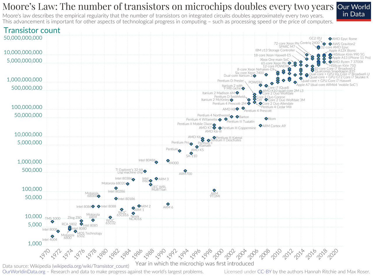
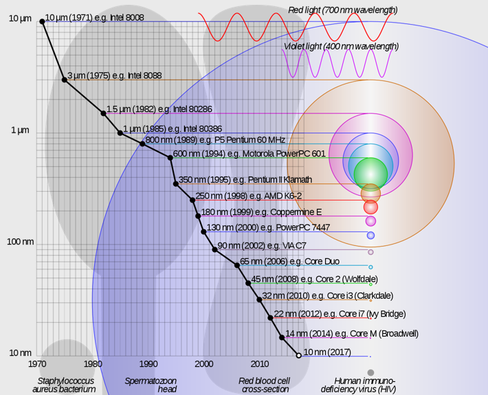
Some leading technologists have claimed Moore’s law is dead; others argue it is still a force. If you are curious to learn more about Moore’s law and associated manufacturing trends in the semiconductor industry, check out the links below:
- (Burg & Ausubel, 2021)
- (Yoshida, 2022)
- (Huang: Moore’s law is dead 2022)
- (Gelsinger: Moore’s law is not dead 2022)
The motto of the real estate industry is “location, location, location,” emphasizing how important location is to present and future property values. In the semiconductor industry the saying is, “faster, smaller, cheaper.” This is driven by Moore’s law and by the ever-increasing expectations of consumers. The end result is a highly competitive market with high barriers to entry and steep operating costs. The miniaturization of electronic components and exponentially increasing transistor counts creates a need for precision and purity in the manufacturing environment.
As one site points out, semiconductor fabrication requires a tremendous amount of water. Fabrication of a 30cm wafer requires up to 2200 gallons of water; a large fabrication facility may easily consume 4.8 million gallons per day. This is average annual water consumption of a city of 60000! And not just any water. Minute contaminants in the water can create impurities and defects in integrated circuits. Therefore water is passed through reverse osmosis several times to produce “ultra pure water.” Ultra pure water is considered an industrial solvent, and it is unsafe to drink. It is so pure, its consumption leeches vital minerals from the body and will eventually kill the consumer. It takes 1400-1600 gallons of municipal water to create 1000 gallons of ultra pure water.
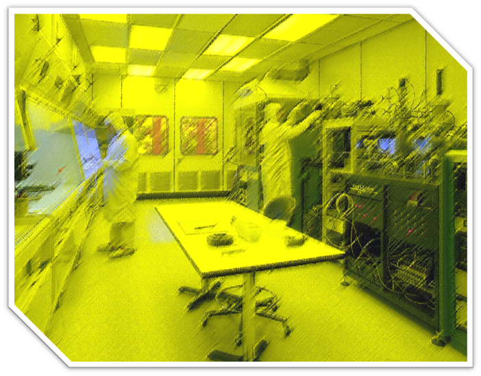
In addition to water, fabrication makes intensive use of other resources. A large manufacturing facility can use 30-50 megawatts during peak production; this is enough to power a small city. Fabrication facilities need to have pressurized chambers, fans, and well-designed air flow patterns to reduce impurities introduced via the air. As part of my work on this project, I was given a tour of a fabrication facility. The tour required wearing the appropriate protective gear to prevent contamination of the manufacturing process. Additionally, the lights in the fabrication rooms were yellow; apparently this spectrum of light is least likely to interact with wafers and components. The intensity of semiconductor manufacturing and the demands of the highly competitive semiconductor market mean production costs must be optimized for a firm to be viable.
As a result of these demands and constraints, rigorous production processes are put in place. Environmental variables are tightly controlled to ensure a robust manufacturing process minimizing errors. Nonetheless, product defects do occur. They must be cataloged and studied to improve the manufacturing process. This endeavor can be costly and time-consuming. Without more sophisticated approaches, the process of categorizing product defects is done through inspection by engineers. Hence a challenge for the manufacturer is how to efficiently classify defective products into defect patterns.
At best an engineer tends to classify one image per minute. There may be thousands of defective products on a product line, and so the defect classification process can take up to two weeks of an engineer’s time for a single product line. An automated approach, has the potential to mitigate this. Ideally, if this can be done with minimal time investment by engineers, it frees up labor for finding solutions to product issues. This frees an engineer to focus on finding sources of product defects and investigating manufacturing process improvements.
Data Set, Similarity Measures, & Data Processing
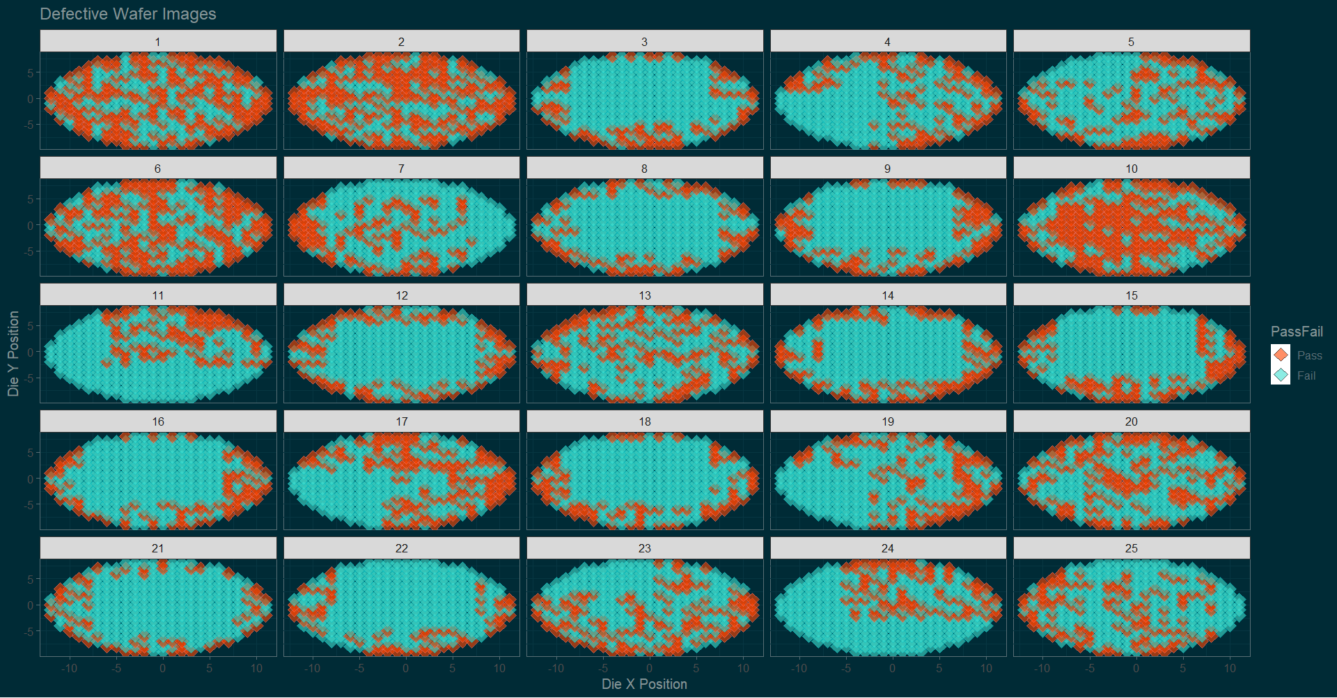
A wafer probe is a testing machine for integrated circuits. The machine’s probe tests each die of a wafer for functionality and electrical conductivity. The wafer is systematically moved under the probe so that once a die has been tested the adjacent die is tested next. The ‘pass’ or ‘fail’ status of each die and die location are stored in a file called a wafer map. This wafer map is a digital representation of the testing results which can then be analyzed. For the purposes of this project, the corporate team shared data samples from a couple product lines (in order to protect privacy). For illustration wafer maps are visualized below with data from a simulation.
To initiate the analysis, we need a mechanism to convert the data representating die passes and fails on each wafer into information about how ‘similar’ each pair of wafers are to eachother. Here the idea of a similarity measure is helpful. In technical terms, a similarity measure is function on a set of objects that returns a number signifying how close those objects are. There is no single form for a similarity measure, though they tend to be the inverse, in some sense of the word, of a distance metric.
As an example take distance (our regular idea of distance, what is called Euclidean distance in math). Distance tells us how far apart two points or two objects at those points are. The negative of the distance can be thought of a similarity index. Close (i.e. similar) objects have a high similarity score (a small negative value in this case) and distant (i.e. dissimilar) objects have a low similarity score (highly negative). Inverse distances like this work great for continuous data. But our data consisted of ‘pass’/’fail’ readings, which are typically converted into binary data - ones and zeros. Hence this project required a binary similarity. A binary similarity is used for observations whose data consists of binary categories - ones and zeros.
There are four basic quantities used in constructing binary similarity measures. These quantities arise from the four possible combinations of ones and zeros. Assume we have two observations labeled \(x\) and \(y\). For each observation we have a set of variables \(x_i\) represented by numbers \(i\). So \(x_1\) is the first variable and \(x_2\) the second for observation \(x_1=1\) might signify that the person is female and \(x_2=1\) may indicate that the person is Rh-positive blood type. Then the four quantities, labeled \(a\), \(b\), \(c\), and \(d\) between two observations \(x\) and \(y\) are:
- \(a\): # of \(i\) where \(x_i=1\) and \(y_i=1\)
- \(b\): # of \(i\) where \(x_i=1\) and \(y_i=0\)
- \(c\): # of \(i\) where \(x_i=0\) and \(y_i=1\)
- \(d\): # of \(i\) where \(x_i=0\) and \(y_i=0\)
Using these quantities there are many ways to build similarities. The simplest is the total percentage of matches: \(\frac{a+d}{a+b+c+d}\). For a comprehensive list of binary similarities see the following studies and references therein:
For the purposes of our study we chose the following similarity formula: \(S=\frac{a+d}{a+b+c}\). To intuitively understand why, note that \(b\) and \(c\) only contribute to denominator. So if all categorical variables are mismatched between \(x\) and \(y\), everything will fall under \(b\)$ or \(c\) and the similarity will be \(0\). \(a\) represents a positive match. So if \(x\) and \(y\) were all ones, we would have a similarity of \(1\). Now if \(x\) and \(y\) were all zeroes, i.e. we have all negative matches, we only have \(d\). In this case the similarity approaches infinity. In practice we would replace infinity with some very large number. This similarity measure is valuing negative matches moreso then positive ones (pun unintended!). In our context a negative match is a match on failing die. As our primary interest is classifying defect patterns, it makes sense to value negative matches the most. Positive matches still count for something over mismatches.
While the sample sizes shared with our team were small, on the order of hundreds of observations, actual product lines could be on the order of hundreds of thousands of wafers or more. So to increase computational efficiency we applied a spectral dimensionality reduction preprocessing step. As long as the similarity measured used is symmetric, the matrix of similarities between wafers will be symmetric, meaning it can be diagonalized and eigenvalues can be obtained. Eigenvalues contain fundamental information about how a matrix is structured and how it functions as a linear operator. By selecting the largest eigenvalues and their associated eigenvectors, a lower dimensional representation of the matrix can be found. The basic code below in R takes an \(n\times{}n\) matrix and converts it into an \(n\times{}m\) dimensional matrix with normalization rows.
Spectra = function(S,t){
  eig = eigen(S,symmetric=TRUE)
  eigvalues = eig$values
  eigvectors = eig$vectors

  m = length(eigvalues[abs(eigvalues)>t])

  U = eigvectors[,1:m]

  for (i in 1:length(U[,1])){
    U[i,]=sqrt((U[i,]^2)/sum(U[i,]^2))
  }

  return(list(eigvalues,eigvectors,U))
}
For a deeper dive into spectral dimensionality reduction, see (Belkin & Niyogi, 2003). From here we were ready to apply a clustering mechanism to identify clusters of wafers based on defect patterns.
Chinese Restaurants and Indian Buffets
The machine learning community typically divides clustering problems into two categories: supervised and unsupervised. In supervised clustering problems, training data has the correct classifications, so we can test a model’s predictions against observed classifications for accuracy. In unsupervised clustering problems the “correct” clusters are not known beforehand, and there may well be no correct answer. Rather we often would like to cluster observations in the most meaningful way. This problem was unsupervised. Furthermore, we do not know how many clusters (i.e. how many product defect patterns) we are looking for beforehand. So this is a latent clustering problem. We need (to get the algorithm) to figure out how many clusters for defect patterns we have and match observations to their most likely cluster.
The Chinese restaurant process refers to a nonparametric Bayesian technique for latent clsutering. The dynamics of the allocation model are said to mimic the pattern of seating at a Chinese restaurant. In this analogy each new observation is assigned to an existing cluster or creates a new cluster, with each possibility having a certain probability. The probability of sitting with any existing cluster is proportional to the number of observations already present in the cluster. A parameter of the model determine the remaining probability of sitting at a new cluster. The Chinese restaurant process analogy was first introduced in the following conference paper: (Aldous 1985).
The Chinese restaurant process is fine in settings where observations are equally likely to sit together (i.e. cluster together). But in this setting, we want to cluster wafers by defect patterns. Wafers with “closer” patterns should ideally have a higher chance of clustering together. Here a distance dependent Chinese restaurant process adds the necessary flexibility of incorporating a distance measure (or in our case a similarity measure) between observations. Observations that are closer will be more likely to sit in the same cluster. The method of the distance dependent Chinese restaurant process was first introduced in (Blei & Frazier, 2011). The model comes with a set of hyperparameters that need to be set. This was automated using a hyperparameter method introduced in (West 1992).
On the data given a total of 5 clusters were identified (and defect patterns subsequently modeled using a Gaussian mixture model). While the company data used for this project is private. The following is the result of simulation test used to validate the method. Wafers conforming to one of four obviously different defect patterns were simulated. All featured heavily defective die in a single quadrant of the wafer. A total of 6 observations were generated in the first category, 2 in the second and third, and 4 in the fourth.
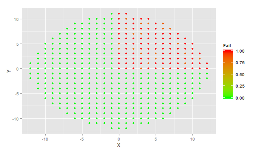
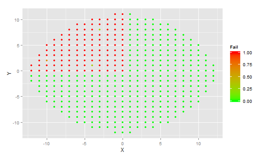
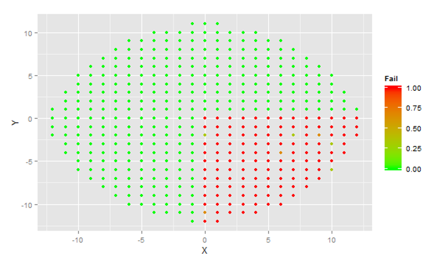
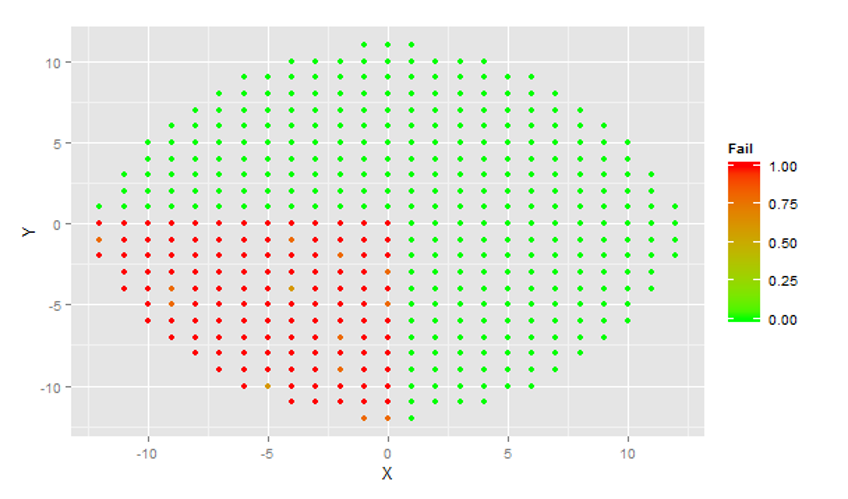
The algorithm correctly identified 4 clusters and correctly classified each simulated wafer in its respective category. The output below was observed:
Output: [1] 3 3 3 3 3 3 1 1 4 4 2 2 2 2
The distance dependent Chinese restaurant offered a framework for latent clustering which worked well on the given data set. However, during the course of the project research, the parallel idea of latent feature analysis. While wafers with distinct patterns can be easily classified into distinct clusters, what if some wafers overlap on some defect patterns but differ on others? Instead of thinking of wafers as falling into clusters of defect patterns, we can think of wafers as having a set of features, in this case defect patterns. Wafers may overlap on some features and differ on others. This provides a more flexible framework as wafers may share some defect features and differ on others. A similar restaurant analogy exists for this latent feature modeling: the Indian buffet process. In this analogy customers (observations) may share some features (e.g. both get chicken vindaloo) but differ on others (e.g. one gets a vegetable samosa, one a lamb korma). The Indian buffet process was first explicated in (Griffiths & Ghahramani, 2005), and a distance dependent Indian buffet process was introduced in (Gershman, Frazier, Blei, 2014).